


Wide band gap semiconductors are extremely attractive for power electronics applications. GaN is a binary III-V wide-band gap ( 3.4 eV) material. Since GaN transistors can operate at much higher temperatures and work at much higher voltages than gallium arsenide (GaAs) transistors, they make ideal power amplifiers at microwave frequencies.
GaN has shown to have applications in optoelectronic, high-power and high-frequency devices. Because GaN offers very high breakdown voltages, high electron mobility, and saturation velocity it is also an ideal candidate for high-power and high-temperature microwave applications like RF power amplifiers at microwave frequencies and high-voltage switching devices for power grids.
GaN devices target both military (ship-board, airborne and ground Radars and high performance space electronics) and commercial applications ( base station transmitters, C-band Satcom, Ku-K band VSAT and broadband satellites, LMDS and digital radio).
There are basically two manufacturing (growth) processes, based on either Silicon or Silicon-Carbide substrates. GaN-on-Si has a significant cost advantage that is driving down the cost curve.
Initially, it seemed GaN-based devices would be affordable only for military applications, such as the development of electronic warfare, radar, and high security communications systems. However, material maturity, improvement in yield, expansion to 4” wafers and lower-cost silicon growth process has reduced GaN-based device costs and therefore an economical option for commercial applications as well.
Growth of the GaN device market has required the development of novel packaging solutions. Since GaN HEMTs are thermally limited significantly below the electrical capability of the devices. The challenge of a GaN HEMT is its heat flux at the gate fingers, which cannot be effectively addressed by conventional packaging and thermal management systems.
The DARPA ICECool program is developing liquid cooling solution for such hot GaN devices. [see IFTLE 119, “ICECool putsThermal Issues Back in Focus”.]
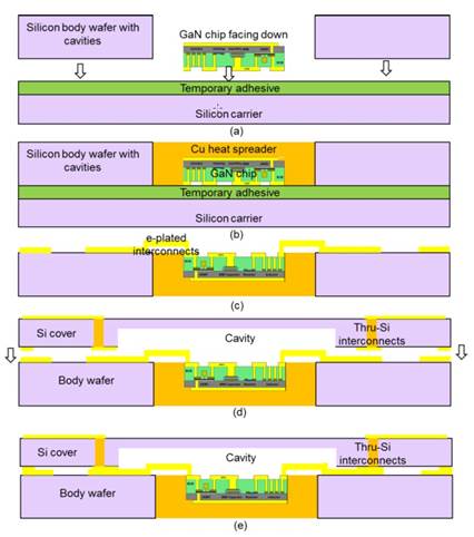
Non liquid cooling solutions are also under development at facilities such as HRL (Hughes Research Labs). While thermal heat spreaders are usually limited by the TIM (thermal interface materials ) used to attach them, The HRL solutions electroplate the heat sink right on the back side of the GaN device or module. For instance see the process sequence below, developed by Herrault and co-workers at the HRL Labs in Malibu CA.
First, GaN dice are temporarily bonded face down onto a carrier wafer using a temporary adhesive layer. The silicon body wafer, which consists of through-wafer cavities, is also bonded face down onto the carrier wafer, as depicted in the figure (a). Next, a Ti/Au seed layer is sputtered over the wafer, and copper is electroplated and subsequently polished down to the surface of the silicon wafer as shown in (b). This step forms the integrated thermal heat spreader. Therefore, there is intimate contact between the high-thermal-conductivity heat spreader and the high-power-density GaN device, which is beneficial for high-performance thermal management. The silicon body wafer was used as a polishing barrier for the copper removal, enabling a flat and smooth backside for additional processing steps. The combination of use of a silicon body wafer, electroplating and chemical mechanical planarization (CMP) process eliminates the need for a bonding layer between the chip and the heat spreader, and therefore reduces the overall thermal resistance from junction to baseplate.
The body wafer with copper-embedded GaN dice is then released from the carrier wafer. Front-side electroplated gold connectors and bond pads are then fabricated using standard microfabrication technologies. The silicon cap with TSV allows connections to the outside of the module.
The technology is compatible with integration of multiple chips (GaN, CMOS, SiGe) from different semiconductor technologies and with different thicknesses since the chip thicknesses are absorbed by the plated copper which is subsequently CMP’ed.

Compared to conventionally mounted GaN power amplifiers (PA) using AuSn solder, an electroformed (called ITAP) X-band PA showed 1.4x improvement in CW Pout (4.4W at 8 GHz) while the ITAP Ku-band showed 1.3x improvement in CW Pout (4W at 12 GHz). Compared to silver epoxy mounted PAs the improvement was 2x and 1.5x, respectively.
The figure below plots Junction temperature vs. dissipated power density using gate resistance test structures. The electroplated heat sinks (ITAP 1 & 2) increase the power handling by 1.45x (for Tj of 150°C) or reduce Tj by 40°C (at 2W/mm dissipated power density).
